Search results for "Resistor

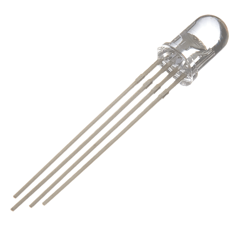
An RGB LED (Red, Green, Blue Light Emitting Diode) is a type of LED that combines three LEDs in one package. Each LED can emit one of the primary colors of light: red, green, or blue. By varying the intensity of each LED, a wide range of colors can be produced. RGB LEDs are commonly used in decorative lighting, displays, and various electronic projects.

Key Features:

  • Combines red, green, and blue LEDs in a single package
  • Can produce a wide range of colors by mixing the three primary colors
  • Common anode or common cathode configurations available
  • Suitable for PWM (Pulse Width Modulation) control
  • Long life and low power consumption
  • Compatible with various microcontroller platforms (e.g., Arduino, Raspberry Pi)

Technical Specifications:

  • Type: RGB LED
  • Package: 5mm or 10mm (varies by product)
  • Configuration: Common Anode or Common Cathode
  • Forward Voltage:
    • Red: 2.0V – 2.2V
    • Green: 3.0V – 3.2V
    • Blue: 3.0V – 3.2V
  • Forward Current: 20mA per color
  • Luminous Intensity:
    • Red: Typically 800 mcd
    • Green: Typically 1500 mcd
    • Blue: Typically 500 mcd
  • Viewing Angle: 30-60 degrees
  • Wavelength:
    • Red: 620-630 nm
    • Green: 515-530 nm
    • Blue: 460-475 nm

Applications:

  • Decorative lighting
  • Displays and indicators
  • RGB color mixing
  • DIY electronics projects
  • Mood lighting
  • Light shows and effects

Usage:

  1. Connection:
    • Identify the anode (longest lead) and the three cathodes (shorter leads) if using a common anode RGB LED, or the cathode (longest lead) and the three anodes if using a common cathode RGB LED.
    • Connect the common lead (anode or cathode) to the appropriate voltage supply or ground.
    • Connect the red, green, and blue leads to the respective control signals or PWM outputs of a microcontroller.
  2. Control:
    • Use digital output pins or PWM signals to control the intensity of each color.
    • Adjust the duty cycle of the PWM signals to mix the colors and produce various hues.
  3. Programming:
    • Write code to control the RGB LED, adjusting the brightness of each color channel to achieve the desired color output.

Caution:

  • Ensure proper current limiting resistors are used to prevent excessive current through the LEDs.
  • Verify the forward voltage and current ratings to avoid damaging the LEDs.
  • Handle the LED carefully to avoid bending the leads or damaging the package.

Datasheet:
For detailed technical specifications, refer to the RGB LED Datasheet.

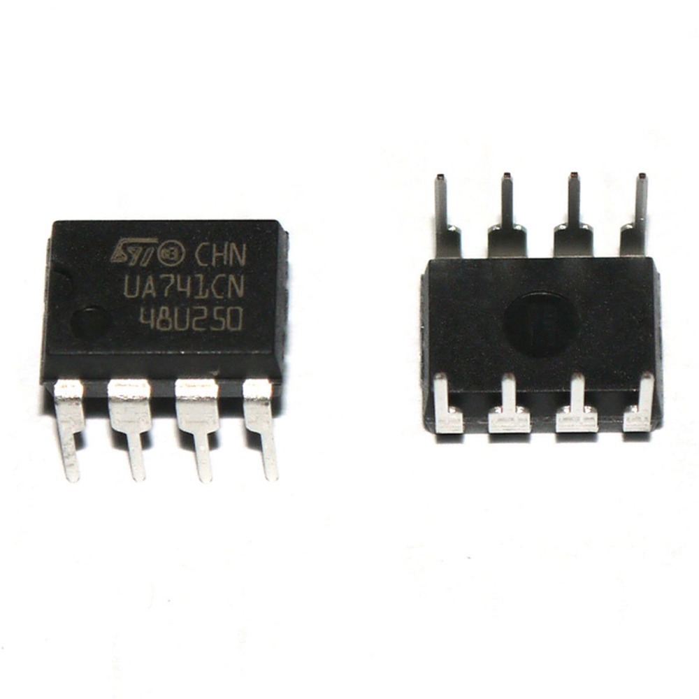
The UA741 is a general-purpose operational amplifier featuring offset-voltage null capability. The high-gain, internally frequency-compensated op-amp is designed to operate from a single or dual power supply over a wide range of voltages. It is an ideal choice for applications requiring low input bias current, low offset voltage, and high input impedance.

Key Features:

  • Internally frequency compensated for unity gain
  • Large signal voltage gain of 106 dB
  • Wide power supply range: ±10V to ±15V
  • Short-circuit protection
  • Offset-voltage null capability
  • Low input bias current: 80 nA (typical)
  • High input impedance: 2 MΩ (typical)
  • Low power consumption
  • Compatible with standard LM741 pin configurations

Technical Specifications:

  • Supply Voltage Range: ±10V to ±22V
  • Input Offset Voltage: 1 mV (typical)
  • Input Bias Current: 80 nA (typical)
  • Input Impedance: 2 MΩ (typical)
  • Output Impedance: 75Ω (typical)
  • Large Signal Voltage Gain: 106 dB (typical)
  • Unity-Gain Bandwidth: 1 MHz (typical)
  • Slew Rate: 0.5 V/µs (typical)
  • Common Mode Rejection Ratio (CMRR): 90 dB (typical)
  • Power Supply Rejection Ratio (PSRR): 96 dB (typical)
  • Operating Temperature Range: 0°C to +70°C
  • Package Types: 8-pin PDIP, SOIC, TO-99

Applications:

  • Signal conditioning
  • Voltage followers
  • Integrators and differentiators
  • Active filters
  • General-purpose analog applications
  • Audio amplifiers
  • Industrial controls
  • Data acquisition systems

Usage:

  1. Connection:
    • Connect the power supply to the V+ and V- pins.
    • Connect the input signal to the inverting (−) or non-inverting (+) input pin.
    • Connect the output to the desired load or next stage of the circuit.
    • Use the offset null pins if necessary to adjust the input offset voltage.
  2. Configuration:
    • Configure the op-amp in the desired configuration (e.g., voltage follower, inverting amplifier, non-inverting amplifier) by connecting the appropriate feedback components.
    • Adjust the gain and frequency response using external resistors and capacitors.
  3. Protection:
    • Use proper decoupling capacitors on the power supply lines to reduce noise and improve stability.
    • Ensure the op-amp is within the recommended supply voltage range to prevent damage.

Caution:

  • Observe proper handling procedures to avoid electrostatic discharge (ESD) damage.
  • Ensure the input signals are within the common-mode voltage range to prevent improper operation.
  • Avoid exceeding the maximum ratings for voltage, current, and temperature.

Datasheet:
For detailed technical specifications, refer to the UA741 Op-Amp Datasheet.

The Nokia 5110 LCD is a basic graphic LCD screen originally intended for use as a cell phone screen. It is a low-cost, easy-to-use display module, perfect for various electronics projects. The LCD features a PCD8544 controller, which can communicate with microcontrollers via an SPI interface.

Key Features:

  • 84 x 48 pixel resolution
  • PCD8544 controller
  • SPI (Serial Peripheral Interface) communication
  • Low power consumption
  • Backlight for enhanced visibility
  • Compact size and lightweight
  • Suitable for text and simple graphics

Technical Specifications:

  • Operating Voltage: 2.7V to 3.3V
  • Current Consumption: 6 mA (with backlight on), 0.5 mA (with backlight off)
  • Display Resolution: 84 x 48 pixels
  • Communication Interface: SPI
  • Backlight: LED backlight (white or blue)
  • Module Dimensions: 43.6mm x 43.1mm
  • Viewing Area: 38mm x 34mm
  • Operating Temperature Range: -20°C to +70°C

Applications:

  • DIY electronics projects
  • Portable devices
  • Wearable electronics
  • User interfaces for embedded systems
  • Educational tools
  • Prototyping and development

Usage:

  1. Connection:
    • Connect the VCC pin to a 3.3V power supply.
    • Connect the GND pin to ground.
    • Connect the SCE (chip enable), RST (reset), D/C (data/command), DN(MOSI) (data input), and SCLK (clock) pins to the corresponding pins on the microcontroller.
    • If using the backlight, connect the LED+ pin to a power supply (usually 3.3V) and the LED- pin to ground through a current-limiting resistor.
  2. Initialization:
    • Initialize the display by sending the appropriate commands to the PCD8544 controller via SPI.
  3. Operation:
    • Use the SPI interface to send data and commands to the display.
    • Draw text and graphics by manipulating the pixels on the screen.
  4. Programming:
    • Write code on the microcontroller to control the display.
    • Many microcontroller platforms, such as Arduino, have libraries available to simplify interfacing with the Nokia 5110 LCD.

Caution:

  • Ensure the supply voltage does not exceed 3.3V to prevent damage to the LCD.
  • Handle the module carefully to avoid damage to the display and pins.
  • Avoid exposing the LCD to excessive heat or moisture.

Datasheet:
For detailed technical specifications, refer to the Nokia 5110 LCD Datasheet.

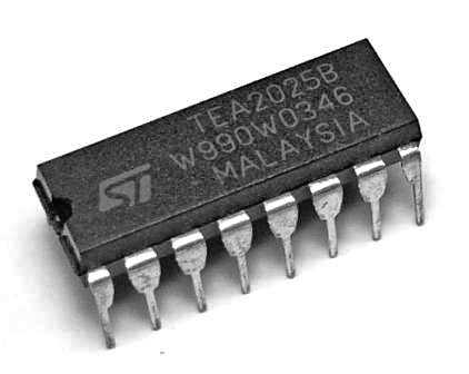
The TEA2025 is a dual audio power amplifier designed for use in portable radio cassette players and other consumer electronics applications. It is capable of delivering 2.5W per channel of continuous output power into 4Ω loads, or 1.5W per channel into 8Ω loads with a 9V supply. The TEA2025 offers low harmonic distortion and good signal-to-noise ratio, making it suitable for high-quality audio amplification.

Key Features:

  • Dual-channel audio amplifier
  • Output power: 2.5W per channel (4Ω), 1.5W per channel (8Ω)
  • Low harmonic distortion
  • High signal-to-noise ratio
  • Internal thermal protection
  • Low quiescent current
  • Few external components required
  • Compact 16-pin dual in-line package (DIP)

Technical Specifications:

  • Operating Voltage: 3V to 15V
  • Output Power:
    • 2.5W per channel into 4Ω (Vcc = 9V)
    • 1.5W per channel into 8Ω (Vcc = 9V)
  • Total Harmonic Distortion: 0.2% (typical)
  • Signal-to-Noise Ratio: 80dB (typical)
  • Gain: 46dB (fixed)
  • Quiescent Current: 8mA (typical)
  • Package Type: 16-pin DIP
  • Operating Temperature Range: -10°C to +70°C

Applications:

  • Portable radio cassette players
  • Consumer electronics
  • Audio amplification in small devices
  • Multimedia speakers
  • Intercom systems

Usage:

  1. Connection:
    • Connect the Vcc pin to a suitable power supply (typically 9V).
    • Connect the ground pin to the system ground.
    • Connect the audio input signals to the input pins.
    • Connect the output pins to the speaker terminals (4Ω or 8Ω).
    • Add necessary external components (e.g., capacitors, resistors) as per the recommended application circuit in the datasheet.
  2. Operation:
    • Apply the audio signal to the input pins.
    • The TEA2025 will amplify the input signal and drive the connected speakers.
  3. Mounting:
    • Ensure proper heat dissipation by mounting the IC on a suitable PCB with adequate thermal management.
    • Use heatsinks if necessary to avoid thermal shutdown during high power operation.

Caution:

  • Ensure the power supply voltage does not exceed the maximum rated voltage to prevent damage to the IC.
  • Handle the IC carefully to prevent damage from electrostatic discharge (ESD).
  • Avoid short-circuiting the output terminals to prevent damage.

Datasheet:
For detailed technical specifications, refer to the TEA2025 Datasheet.

Category: Analog Audio Amplifier

595 Shift Register

Description:
The 74HC595 is an 8-bit serial-in, parallel-out shift register with an 8-bit storage register. The device features a serial data input (DS), eight parallel data outputs (Q0-Q7), and a serial output for cascading (Q7′). It is commonly used to expand the number of I/O pins available on a microcontroller, enabling control of multiple outputs with a few pins.

Key Features:

  • 8-bit serial-in, parallel-out shift register
  • 8-bit storage register with tri-state outputs
  • Serial input (DS) and serial output for cascading (Q7′)
  • Three-state outputs (Q0-Q7)
  • Low power consumption
  • High-speed operation
  • Cascadable with multiple 74HC595 ICs

Technical Specifications:

  • Operating Voltage: 2V to 6V
  • Maximum Clock Frequency: 100 MHz (at Vcc = 4.5V to 5.5V)
  • Current Consumption: 80 μA (maximum, at Vcc = 6V)
  • Output Current per Pin: 35 mA (maximum)
  • Total Current through Vcc/GND: 70 mA (maximum)
  • Propagation Delay Time: 23 ns (at Vcc = 5V)
  • Package Types: 16-pin PDIP, SOIC, TSSOP
  • Operating Temperature Range: -40°C to +125°C

Applications:

  • LED displays
  • Keypad interfaces
  • Data acquisition systems
  • Digital signal processing
  • Memory addressing
  • Control systems

Usage:

  1. Connection:
    • Connect the Vcc pin to a 5V power supply (or appropriate voltage within the operating range).
    • Connect the GND pin to ground.
    • Connect the serial data input (DS) to the microcontroller’s data output pin.
    • Connect the clock input (SH_CP) and latch input (ST_CP) to the microcontroller’s clock and latch control pins.
    • Connect the parallel outputs (Q0-Q7) to the desired peripheral devices.
    • Use the serial output (Q7′) to cascade additional 74HC595 shift registers if needed.
  2. Operation:
    • Send serial data to the DS pin while providing clock pulses to SH_CP.
    • Latch the data to the output pins by providing a pulse to the ST_CP pin.
    • Control multiple 74HC595 ICs in series by connecting the Q7′ of one to the DS of the next.
  3. Programming:
    • Write code on the microcontroller to control the shift register.
    • Shift in data bits and latch them to update the outputs as needed.

Caution:

  • Ensure the supply voltage does not exceed the maximum rated voltage to avoid damage to the IC.
  • Handle the IC carefully to prevent damage from electrostatic discharge (ESD).
  • Avoid exceeding the maximum current ratings to prevent overheating and damage.

Datasheet:
For detailed technical specifications, refer to the 74HC595 Datasheet.

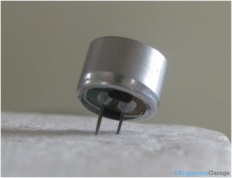
The Condenser Mic 4.5×2.2mm is a small-sized, high-sensitivity electret microphone. It is designed for a wide range of audio applications, including voice recording, telecommunication devices, and various consumer electronics. Its compact size and high sensitivity make it ideal for embedding in small devices.

Key Features:

  • High sensitivity and low noise
  • Small and compact size
  • Wide frequency response
  • Low power consumption
  • Omnidirectional pickup pattern
  • Easy to integrate into electronic circuits

Technical Specifications:

  • Type: Electret condenser microphone
  • Dimensions: 4.5mm (diameter) x 2.2mm (height)
  • Sensitivity: -42dB ±3dB (0dB = 1V/Pa at 1kHz)
  • Frequency Response: 20Hz to 16kHz
  • Impedance: ≤ 2.2kΩ
  • Operating Voltage: 1.5V to 10V DC
  • Current Consumption: ≤ 0.5mA
  • Signal-to-Noise Ratio: ≥ 60dB
  • Directivity: Omnidirectional
  • Operating Temperature Range: -20°C to +70°C

Applications:

  • Voice recording devices
  • Telecommunication equipment
  • Hearing aids
  • Portable audio recorders
  • Consumer electronics
  • Smart home devices
  • Speech recognition systems

Usage:

  1. Connection:
    • Connect the microphone’s output pin to the input of an amplifier or preamp circuit.
    • Connect the power supply (1.5V to 10V DC) to the microphone.
    • Ensure the ground connection is properly made to avoid noise interference.
  2. Integration:
    • Place the microphone in a suitable location to capture sound effectively.
    • Embed the microphone in devices ensuring the sound entry is not obstructed.
  3. Circuit Design:
    • Use appropriate capacitors and resistors as per the microphone’s requirements.
    • Design the circuit to provide a stable power supply and proper impedance matching.

Caution:

  • Handle the microphone with care to avoid physical damage.
  • Protect the microphone from exposure to moisture and extreme temperatures.
  • Avoid applying excessive voltage to prevent damage to the microphone.

Datasheet:
For detailed technical specifications, refer to the Condenser Microphone Datasheet.

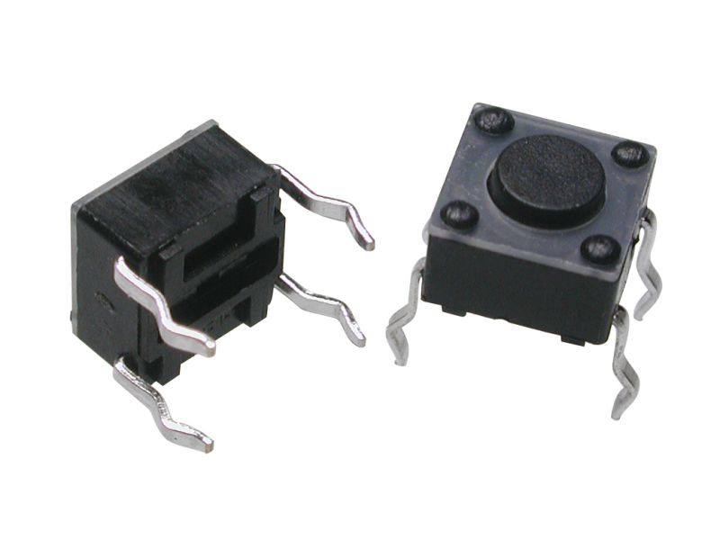
A Tact Switch, also known as a tactile switch, is a type of switch designed to provide a tactile feedback when pressed. These switches are commonly used in electronic devices for user input, such as in keyboards, remote controls, and various consumer electronics. Tact switches are known for their compact size, reliability, and ease of integration into circuits.

Key Features:

  • Tactile Feedback: Provides a satisfying click feel when pressed.
  • Compact Size: Small and suitable for space-constrained applications.
  • Reliability: Durable and designed for a high number of actuation cycles.
  • Variety of Sizes: Available in different sizes and heights to fit various designs.
  • Easy Mounting: Can be mounted on PCBs with through-hole or surface-mount technology.
  • Wide Application Range: Suitable for a variety of electronic devices and applications.

Technical Specifications:

  • Contact Rating: Typically 50mA, 12V DC
  • Contact Resistance: ≤ 100mΩ
  • Insulation Resistance: ≥ 100MΩ at 100V DC
  • Dielectric Strength: 250V AC for 1 minute
  • Operating Force: Typically 160gf (varies by model)
  • Travel: Typically 0.25mm to 0.5mm
  • Operating Life: Typically 100,000 to 1,000,000 cycles
  • Operating Temperature Range: -20°C to +70°C

Applications:

  • Consumer Electronics: Used in remote controls, calculators, and gaming controllers.
  • Computer Peripherals: Keyboards, mice, and other input devices.
  • Home Appliances: Control panels for microwaves, washing machines, and other appliances.
  • Automotive: Control buttons on car dashboards and steering wheels.
  • Industrial Equipment: Control panels and user interfaces for machinery.
  • DIY Projects: Suitable for custom electronic projects and prototypes.

Usage:

  1. Mounting: Solder the tact switch onto a PCB, ensuring correct alignment of the pins.
  2. Wiring: Connect the switch to your circuit, typically using pull-up or pull-down resistors.
  3. Testing: Verify the switch functionality by pressing it and checking the response in your circuit.
  4. Integration: Integrate the switch into your final product, ensuring it is accessible and functions as intended.

Caution:

  • Debouncing: Implement debouncing in your software to ensure accurate readings.
  • Proper Soldering: Avoid excessive heat during soldering to prevent damage to the switch.
  • Environmental Conditions: Ensure the switch is used within its specified temperature and humidity range.

Datasheet:
For detailed technical specifications, refer to the Tact Switch Datasheet.

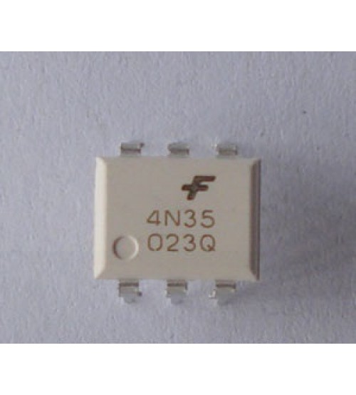
The 4N35 is a general-purpose optocoupler that consists of an infrared LED and a silicon phototransistor. It is designed to provide electrical isolation between input and output circuits while allowing signal transmission. This optocoupler is widely used in applications requiring noise isolation, signal isolation, and interface compatibility between high voltage and low voltage systems.

Key Features:

  • High isolation voltage (typically 5,000 Vrms)
  • Fast switching speed
  • Low input current requirements
  • Wide operating temperature range
  • Compact and reliable design
  • Compatible with various digital and analog circuits

Technical Specifications:

  • Isolation Voltage: 5,000 Vrms (min)
  • Input LED Forward Voltage: 1.2V (typ), 1.5V (max)
  • Input LED Forward Current: 10mA (typ), 60mA (max)
  • Collector-Emitter Voltage (VCEO): 30V (max)
  • Collector Current (IC): 50mA (max)
  • Current Transfer Ratio (CTR): 20% to 300% (at IF = 10mA, VCE = 5V)
  • Rise Time (tr): 3µs (typ)
  • Fall Time (tf): 2µs (typ)
  • Package Type: 6-pin DIP
  • Operating Temperature Range: -55°C to +100°C

Applications:

  • Signal isolation in communication systems
  • Switching power supplies
  • Microcontroller interface isolation
  • Motor control circuits
  • Industrial automation systems
  • Data acquisition systems

Usage:

  1. Circuit Design:
    • Connect the anode of the input LED to the control signal source and the cathode to the ground, through a current-limiting resistor.
    • Connect the collector of the phototransistor to the load or the microcontroller input, and the emitter to the ground.
  2. Current Limiting:
    • Calculate and use an appropriate current-limiting resistor for the LED input to ensure it operates within the specified current range.
  3. Isolation:
    • Ensure that the input and output sides of the optocoupler are properly isolated to prevent electrical interference and maintain safety.
  4. Testing:
    • Verify the functionality of the optocoupler by applying a control signal to the LED input and observing the output response.

Caution:

  • Handle the optocoupler with care to avoid damage from electrostatic discharge (ESD).
  • Verify the electrical ratings and ensure the device operates within specified limits to avoid damage.
  • Keep the input and output circuits isolated to maintain the integrity of the isolation barrier.

Datasheet:
For detailed technical specifications, refer to the 4N35 Datasheet.

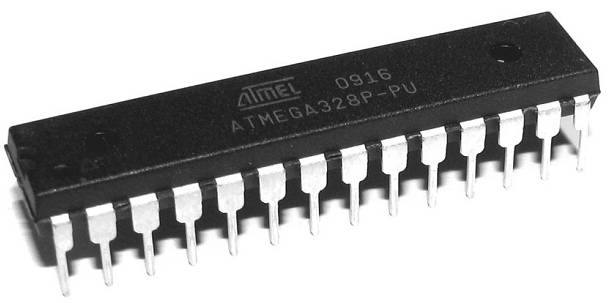
The Atmega 328P-PU is a high-performance, low-power 8-bit AVR microcontroller from Microchip Technology, commonly used in Arduino boards like the Arduino Uno. It features advanced RISC architecture with 32KB of ISP flash memory, 2KB of SRAM, and 1KB of EEPROM. This microcontroller is suitable for a wide range of applications, including embedded systems, consumer electronics, and DIY electronics projects.

Key Features:

  • Advanced RISC architecture
  • 32KB of in-system self-programmable flash memory
  • 2KB SRAM and 1KB EEPROM
  • 23 general-purpose I/O lines
  • 32 general-purpose working registers
  • Three flexible timer/counters with compare modes
  • Internal and external interrupts
  • Serial programmable USART
  • Master/slave SPI serial interface
  • On-chip analog comparator
  • 10-bit ADC with 6 multiplexed channels
  • Operating voltage range of 1.8V to 5.5V
  • Low power consumption in active and sleep modes

Technical Specifications:

  • Architecture: 8-bit AVR
  • Flash Memory: 32KB
  • SRAM: 2KB
  • EEPROM: 1KB
  • Clock Speed: Up to 20 MHz (with external crystal)
  • Operating Voltage: 1.8V to 5.5V
  • Digital I/O Pins: 23
  • PWM Channels: 6
  • Analog Input Channels: 6
  • ADC Resolution: 10-bit
  • Timers: 1 x 16-bit, 2 x 8-bit
  • Communication Interfaces: USART, SPI, I2C
  • Package Type: PDIP-28 (Plastic Dual In-line Package)
  • Operating Temperature Range: -40°C to +85°C

Applications:

  • Arduino development boards
  • Consumer electronics
  • Embedded systems
  • Robotics
  • Home automation
  • DIY electronics projects
  • Industrial automation

Usage:

  1. Programming:
    • Use an AVR programmer or Arduino board to program the Atmega 328P-PU.
    • Commonly programmed using the Arduino IDE for ease of use.
    • Connect the microcontroller to your development environment using the appropriate hardware and software tools.
  2. Circuit Design:
    • Integrate the Atmega 328P-PU into your circuit with necessary external components like crystal oscillators, capacitors, and resistors.
    • Ensure proper power supply and grounding for stable operation.
  3. Interfacing:
    • Utilize the I/O pins for interfacing with sensors, actuators, displays, and other peripherals.
    • Use communication interfaces like USART, SPI, and I2C for data exchange with other devices.

Caution:

  • Handle the microcontroller with care to avoid damage from electrostatic discharge (ESD).
  • Ensure proper power supply voltage and connections to prevent damage.
  • Follow the manufacturer’s guidelines for programming and operation.

Datasheet:
For detailed technical specifications, refer to the Atmega 328P Datasheet.

0

TOP

X