Subtotal: ₦2,510.00
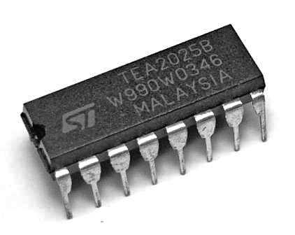
TEA2025 2.5W Analog Audio amplifier
₦200.00
The TEA2025 is a dual audio power amplifier designed for use in portable radio cassette players and other consumer electronics applications. It is capable of delivering 2.5W per channel of continuous output power into 4Ω loads, or 1.5W per channel into 8Ω loads with a 9V supply. The TEA2025 offers low harmonic distortion and good signal-to-noise ratio, making it suitable for high-quality audio amplification.
Key Features:
- Dual-channel audio amplifier
- Output power: 2.5W per channel (4Ω), 1.5W per channel (8Ω)
- Low harmonic distortion
- High signal-to-noise ratio
- Internal thermal protection
- Low quiescent current
- Few external components required
- Compact 16-pin dual in-line package (DIP)
Technical Specifications:
- Operating Voltage: 3V to 15V
- Output Power:
- 2.5W per channel into 4Ω (Vcc = 9V)
- 1.5W per channel into 8Ω (Vcc = 9V)
- Total Harmonic Distortion: 0.2% (typical)
- Signal-to-Noise Ratio: 80dB (typical)
- Gain: 46dB (fixed)
- Quiescent Current: 8mA (typical)
- Package Type: 16-pin DIP
- Operating Temperature Range: -10°C to +70°C
Applications:
- Portable radio cassette players
- Consumer electronics
- Audio amplification in small devices
- Multimedia speakers
- Intercom systems
Usage:
- Connection:
- Connect the Vcc pin to a suitable power supply (typically 9V).
- Connect the ground pin to the system ground.
- Connect the audio input signals to the input pins.
- Connect the output pins to the speaker terminals (4Ω or 8Ω).
- Add necessary external components (e.g., capacitors, resistors) as per the recommended application circuit in the datasheet.
- Operation:
- Apply the audio signal to the input pins.
- The TEA2025 will amplify the input signal and drive the connected speakers.
- Mounting:
- Ensure proper heat dissipation by mounting the IC on a suitable PCB with adequate thermal management.
- Use heatsinks if necessary to avoid thermal shutdown during high power operation.
Caution:
- Ensure the power supply voltage does not exceed the maximum rated voltage to prevent damage to the IC.
- Handle the IC carefully to prevent damage from electrostatic discharge (ESD).
- Avoid short-circuiting the output terminals to prevent damage.
Datasheet:
For detailed technical specifications, refer to the TEA2025 Datasheet.
Category: Analog Audio Amplifier
595 Shift Register
Description:
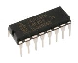
The 74HC595 is an 8-bit serial-in, parallel-out shift register with an 8-bit storage register. The device features a serial data input (DS), eight parallel data outputs (Q0-Q7), and a serial output for cascading (Q7′). It is commonly used to expand the number of I/O pins available on a microcontroller, enabling control of multiple outputs with a few pins.
Key Features:
- 8-bit serial-in, parallel-out shift register
- 8-bit storage register with tri-state outputs
- Serial input (DS) and serial output for cascading (Q7′)
- Three-state outputs (Q0-Q7)
- Low power consumption
- High-speed operation
- Cascadable with multiple 74HC595 ICs
Technical Specifications:
- Operating Voltage: 2V to 6V
- Maximum Clock Frequency: 100 MHz (at Vcc = 4.5V to 5.5V)
- Current Consumption: 80 μA (maximum, at Vcc = 6V)
- Output Current per Pin: 35 mA (maximum)
- Total Current through Vcc/GND: 70 mA (maximum)
- Propagation Delay Time: 23 ns (at Vcc = 5V)
- Package Types: 16-pin PDIP, SOIC, TSSOP
- Operating Temperature Range: -40°C to +125°C
Applications:
- LED displays
- Keypad interfaces
- Data acquisition systems
- Digital signal processing
- Memory addressing
- Control systems
Usage:
- Connection:
- Connect the Vcc pin to a 5V power supply (or appropriate voltage within the operating range).
- Connect the GND pin to ground.
- Connect the serial data input (DS) to the microcontroller’s data output pin.
- Connect the clock input (SH_CP) and latch input (ST_CP) to the microcontroller’s clock and latch control pins.
- Connect the parallel outputs (Q0-Q7) to the desired peripheral devices.
- Use the serial output (Q7′) to cascade additional 74HC595 shift registers if needed.
- Operation:
- Send serial data to the DS pin while providing clock pulses to SH_CP.
- Latch the data to the output pins by providing a pulse to the ST_CP pin.
- Control multiple 74HC595 ICs in series by connecting the Q7′ of one to the DS of the next.
- Programming:
- Write code on the microcontroller to control the shift register.
- Shift in data bits and latch them to update the outputs as needed.
Caution:
- Ensure the supply voltage does not exceed the maximum rated voltage to avoid damage to the IC.
- Handle the IC carefully to prevent damage from electrostatic discharge (ESD).
- Avoid exceeding the maximum current ratings to prevent overheating and damage.
Datasheet:
For detailed technical specifications, refer to the 74HC595 Datasheet.
In stock
Additional Information
| Weight | 0.00148 kg |
|---|

