- You have no items in your shopping cart
- Subtotal: ₦0.00
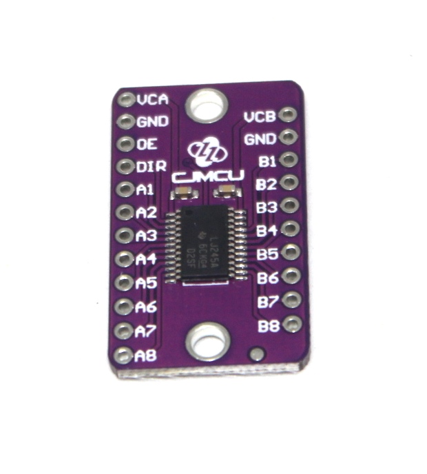
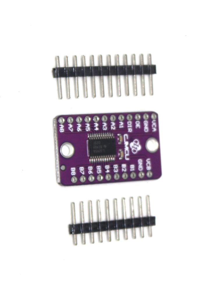
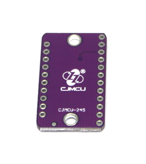
SN74LVC4245A LJ245A octal bus tranciever shifter board
₦5,200.00
Description:
The SN74LVC4245A LJ245A Octal Bus Transceiver Shifter Board is designed for bidirectional voltage-level translation and signal buffering. It is capable of interfacing between different logic levels, making it an ideal choice for mixed-voltage systems. This module supports 8-bit data bus communication and provides efficient signal transmission and reception.
Key Features:
- 8-Bit Bidirectional Transceiver: Enables data transfer between buses
- Voltage-Level Shifting: Interfaces between different logic levels (e.g., 5.5V on A port and 2.7V to 3.6V on B port)
- High-Speed Operation: Ensures fast data transfer rates
- Direction Control: Selects the direction of data flow
- Compact Design: Easy to integrate into various applications
Technical Specifications:
- Operating Voltage: 4.5V to 5.5V (A port), 2.7V to 3.6V (B port)
- Bus Width: 8-bit
- Data Rate: Up to 100 Mbps
- Input/Output Type: 3-state
- Operating Temperature Range: -40°C to +85°C
- Dimensions: Compact board size suitable for integration
Applications:
- Mixed-Voltage Systems: Interfaces between different logic level circuits
- Microcontroller Interfacing: Connects microcontrollers with peripherals operating at different voltages
- Signal Buffering: Enhances signal integrity over long distances
- Embedded Systems: Used in various embedded applications for reliable data communication
Datasheet:
For detailed technical information and specifications, please refer to the SN74LVC4245A LJ245A Octal Bus Transceiver Shifter Board Datasheet.
In stock
This 8-bit (octal) noninverting bus transceiver
contains two separate supply rails; B port has VCCB,
which is set at 3.3 V, and A port has VCCA, which is
set at 5 V. This allows for translation from a 3.3-V to
a 5-V environment, and vice versa.
The SN74LVC4245A device is designed for
asynchronous communication between data buses.
The device transmits data from the A bus to the B
bus or from the B bus to the A bus, depending on the
logic level at the direction-control (DIR) input. The
output-enable (OE) input can be used to disable the
device so the buses are effectively isolated. The
control circuitry (DIR, OE) is powered by VCCA.
The SN74LVC4245A device terminal out allows the
designer to switch to a normal all-3.3-V or all-5-V 20-
terminal SN74LVC4245 device without board relayout. The designer uses the data paths for pins
2–11 and 14–23 of the SN74LVC4245A device to
align with the conventional ‘245 terminal out.
Technical Specifications:
• Bidirectional Voltage Translator
• 5.5 V on A Port and 2.7 V to 3.6 V on B Port
• Control Inputs VIH/VIL Levels Are Referenced to
VCCA Voltage
• Latch-Up Performance Exceeds 250 mA Per
JESD 17
• ESD Protection Exceeds JESD 22
– 2000-V Human-Body Model
– 200-V Machine Model
– 1000-V Charged-Device Model
Applications
• ATCA Solutions
• CPAP Machines
• Cameras: Surveillance Analog
• Chemical or Gas Sensors
• CT Scanners
• DLP 3D Machine Vision and Optical Networking
• Digital Signage
• ECGs: Electrocardiograms
• Field Transmitters: Pressure Sensors and
Temperature Sensors
• High-Speed Data Acquisition and Generation
• HMI (Human Machine Interface)
• RF4CE Remote Controls
• Server Motherboards
• Software Defined Radios (SDR)
• Wireless LAN Cards and Data Access Cards
• X-ray: Medical, Dental, and Baggage Scanners

