Subtotal: ₦36,375.00
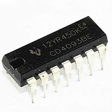
CD4093 Logic Gate and inverter
₦400.00
The CD4093 is a CMOS logic IC that integrates four independent Schmitt trigger circuits within a single package. Each Schmitt trigger circuit in the CD4093 performs the function of a 2-input NAND gate with Schmitt trigger action. This means it converts noisy digital input signals into clean digital outputs with hysteresis, improving noise immunity and signal integrity. The CD4093 operates with low power consumption, high noise immunity, and can function over a wide range of supply voltages.
Key Features:
- Four independent Schmitt trigger circuits (2-input NAND gates)
- Wide supply voltage range: 3V to 15V
- Low power consumption
- High noise immunity
- Buffered inputs and outputs for improved signal integrity
- TTL-compatible inputs
- Hysteresis typically 800mV at VDD = 5V
Technical Specifications:
- Supply Voltage (VDD): 3V to 15V
- Input Voltage Range: 0V to VDD
- High-Level Output Voltage (VOH): VDD – 0.05V (min at VDD = 5V)
- Low-Level Output Voltage (VOL): 0.05V (max at VDD = 5V)
- High-Level Input Voltage (VIH): 70% of VDD (min)
- Low-Level Input Voltage (VIL): 30% of VDD (max)
- Propagation Delay Time: 60 ns (typical at VDD = 10V)
- Operating Temperature Range: -55°C to +125°C
- Package: 14-pin DIP, SOIC
Applications:
- Digital Logic Circuits: Used in digital circuits for implementing NAND logic functions with hysteresis.
- Signal Conditioning: Suitable for cleaning up noisy signals and improving signal integrity.
- Waveform Shaping: Used in circuits requiring stable switching thresholds and noise filtering.
- Oscillators and Timers: Ideal for generating timing signals and square wave oscillations.
- Triggering Circuits: Used in circuits requiring precise triggering based on input voltage levels.
- Data Routing: Suitable for routing digital signals based on NAND logic conditions.
Datasheet:
For detailed technical information, refer to the CD4093 Datasheet.
In stock
Additional Information
| Weight | 0.001125 kg |
|---|
Be the first to review “CD4093 Logic Gate and inverter”
You must be <a href="https://hub360.com.ng/my-account-3/">logged in</a> to post a review.








Reviews
There are no reviews yet.