Subtotal: ₦500.00
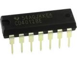
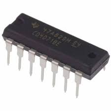
CD4071 buffer/logic chip
₦400.00
The CD4071 is a CMOS logic IC that contains four independent 2-input OR gates. Each gate performs the Boolean function Y = A + B in positive logic, providing standard OR gate functionality. The CD4071 is designed for use in a wide range of digital applications, thanks to its high noise immunity, low power consumption, and wide operating voltage range.
Key Features:
- Four independent 2-input OR gates
- Wide supply voltage range: 3V to 15V
- Low power consumption
- High noise immunity
- Standardized symmetrical output characteristics
- Buffered inputs and outputs for improved signal integrity
- TTL-compatible inputs
Technical Specifications:
- Supply Voltage (VDD): 3V to 15V
- Input Voltage Range: 0V to VDD
- High-Level Output Voltage (VOH): VDD – 0.05V (min at VDD = 5V)
- Low-Level Output Voltage (VOL): 0.05V (max at VDD = 5V)
- High-Level Input Voltage (VIH): 70% of VDD (min)
- Low-Level Input Voltage (VIL): 30% of VDD (max)
- Propagation Delay Time: 60 ns (typical at VDD = 10V)
- Operating Temperature Range: -55°C to +125°C
- Package: 14-pin DIP, SOIC
Applications:
- Digital Logic Circuits: Used in digital circuits for implementing OR logic functions.
- Signal Processing: Suitable for combining digital signals.
- Logic Level Conversion: Employed in circuits requiring conversion between different logic levels.
- Control Systems: Used in control systems requiring logical OR operations.
- Data Routing: Ideal for routing digital signals based on logical conditions.
- Timing Circuits: Implemented in timing circuits for various digital applications.
Datasheet:
For detailed technical information, refer to the CD4071 Datasheet.
In stock
Additional Information
| Weight | 0.001008 kg |
|---|
Be the first to review “CD4071 buffer/logic chip”
You must be <a href="https://hub360.com.ng/my-account-3/">logged in</a> to post a review.




Reviews
There are no reviews yet.