- You have no items in your shopping cart
- Subtotal: ₦0.00
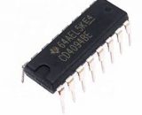
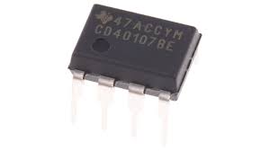
CD40107
₦550.00
The CD40107 is a dual 2-input NAND buffer featuring high output drive capability and low power consumption. It can be used to interface with TTL and other logic families. The device is constructed with complementary MOS (CMOS) technology, ensuring high noise immunity and low static power consumption. It is widely used in digital circuits requiring high current drive and buffering capabilities.
Key Features:
- Dual 2-input NAND buffer
- High output drive capability
- Low power consumption
- High noise immunity
- Wide supply voltage range: 3V to 15V
- Compatible with TTL logic levels
- Buffered outputs for improved signal integrity
Technical Specifications:
- Supply Voltage (VDD): 3V to 15V
- Input Voltage Range: 0V to VDD
- High Level Output Current: -4.2mA (VDD = 5V), -10.5mA (VDD = 10V)
- Low Level Output Current: 8.4mA (VDD = 5V), 21mA (VDD = 10V)
- Operating Temperature Range: -55°C to +125°C
- Package: 14-pin DIP, SOIC
Applications:
- Digital Circuits: Used as a buffer and driver in various digital circuits.
- Interfacing Logic Levels: Interfaces CMOS logic levels with TTL and other logic families.
- Signal Conditioning: Buffers and conditions signals to ensure reliable transmission.
- Industrial Control Systems: Used in control systems for signal buffering and driving high-current loads.
- Consumer Electronics: Implemented in consumer devices requiring high-current drive capabilities.
- Communication Systems: Used in communication systems for signal integrity and buffering.
Datasheet:
For detailed technical information, refer to the CD40107 Datasheet.
In stock
Be the first to review “CD40107”
You must be <a href="https://hub360.com.ng/my-account-3/">logged in</a> to post a review.


Reviews
There are no reviews yet.