Subtotal: ₦18,500.00
Hey there guys, it’s your hardware friend Kayode and today we will be unboxing the functionalities of a shift register. The shift register we will be using is the SN74HC595 from Texas instruments.
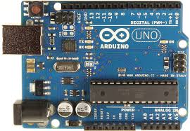
As you build exciting projects with the arduino, you might already be thinking: “What happens when I run out of pins?”. Blinking of LEDs in various patterns seems to be the most popular project implemented on the arduino platform. The most popular arduino board the UNO might not be able to cater for your needs when you want to blink lots of LEDs. This is where shift registers can come in handy. With shift registers, you can expand the I/O capabilities of your Arduino without having to pay a whole lot more for a more expensive board such as the arduino MEGA with additional I/O pins. In this tutorial, we will learn how shift registers work, and you’ll implement both the software and hardware necessary to interface your arduino with shift registers for the purpose of expanding digital output capabilities of the arduino.
The 74HC595 contains a serial in parallel out (SIPO) shift register . This means that it accepts a stream of serial bits and outputs them simultaneously.
In our last tutorial, we turned an LED on using the digitalWrite() function when a command was received from the remote. Suppose that we were to turn on eight LEDs with eight digital outputs; all the bits would be transmitted on independent I/O pins at roughly the same time. This is a parallel transmission and it requires more pins. The shift register only requires three digital pins to output the serial data coming from the arduino.
74HC595 SHIFT REGISTER
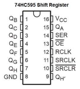
The 74HC595 shift register is a device that makes it easy to convert between serial and parallel data transmission techniques. Its pin out is shown below.
FEATURES
- 8-bit serial in parallel-out shift
- Wide operating voltage range of 2V to 6V
- Shift Register has direct clear
- Low input current: 1μA(maximum)
PIN FUNCTIONS
QA-QH: These are the parallel output pins that will be connected to the LEDs or any other device we want to control
Vcc : This pin is connected to 5V
GND : This is connected to a common ground with the arduino.
SER: This pin receives the 8 sequential bit values coming from the arduino and uses it to set the value of the parallel outputs.
RCLK: This pin is also known as the LATCH pin or register clock pin. When pulled high, it shifts this serial values to the parallel outputs all at once
SRCLK: When this pin goes high, the values in the shift register shift by 1 bit. It will be pulsed eight times to pull in all the data that you are sending on the serial data pin.
QH’: This pin is used to shift serial data to another shift register.
SRCLR: This pin is an active low pin which when pulled low sets all the bits of the parallel output to 0.
OE: The output enable pin enables the parallel output when pulled to ground and disables it when pulled high.
PRINCIPLE OF OPERATION
The 74HC595 shift register is a synchronous device; it is clock-driven on rising edge or only acts on the rising edge of the clock signal. Every time the clock signal transitions from low to high, all the values currently stored in the eight output registers are shifted over one position. Simultaneously, the value currently on the DATA input is shifted into the first position. By doing this eight times, the present values are shifted out and the new values are shifted into the register. When a data is to be sent, the LATCH pin as to be pulled LOW until all the bits are stored in the storage register. After storage the LATCH pin is then pulled HIGH so as to commit the data to the output.
SHIFTING SERIAL DATA FROM THE ARDUINO TO THE SHIFT REGISTER
The arduino IDE has a function which can help us to easily shift out serial data to the 74HC595 shift register. This function is known as the shiftOut() function. It helps to easily shift out 8 bits of data onto an arbitrary I/O pin. It accepts four parameters:
- The data pin number
- The clock pin number
- The bit order
- The value to shift out
Examine how the function is used below:
shiftOut(DATA, CLOCK, LSBFIRST, B1111111);
The DATA and CLOCK constants are set to the pin numbers to the pin numbers physically connected to the arduino.
LSBFIRST indicates that the least significant bit will be sent first (the rightmost bit when looking at the binary number to send). We can also send the data with the LSBFIRST setting, which would start by sending the bits from the left side of the binary data. The last parameter is the number to be sent. By putting a capital B before the number, you are telling the arduino IDE
to interpret the following numbers as a binary value rather than as a decimal integer. Decimals can also be sent. The binary number B11111111 will be 255 in decimal and 0XFF in hexadecimal.
COMPONENTS
We will need the following components in order to do this tutorial
- Arduino uno
- Breadboard
- 74HC595
- LED(8)
- 220R resistor(8)
CIRCUIT DIAGRAM
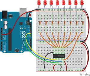
The connection between the arduino and shift register is straight forward and easy to understand. The three pin needed for communication are connected as follows;
- The DATA pin will connect to pin 8.
- The LATCH pin will connect to pin 9.
- The CLOCK pin will connect to pin 10.
The eight LEDs to be controlled are connected to the output pins QA-QH of the shift register.
CODE
As usual, we will break down the code. The code is quite simple and easy to understand
First, we declare and initialize the pins which our serial data, latch and clock will be connected to.
const int SER =8; //Serial output to shift register
const int LATCH =9; //Shift register latch pin
const int CLK =10; //Shift register clock pin
Next we declare an array to store the on and off values. We have earlier discussed how to use binary numbers in the shiftout() function. Since variety is the spice of life we will be using decimals in this code. We used an array to hold the values. An array is a collection of variables that are accessed with an index number. This is array size is two. Arrays are zero indexed therefore its index value will be 0, 1 and 2 with 0 and1 representing 255 and 0 respectively and 2 holding the null character.
int pattern[2] = {255,0}; // array to hold on and off values
In the setup() function, we set pins 8, 9 and 10 of the arduino as an ouput so that it can communicate with the shift register. Recall the shift register receives command from the arduino so it is the slave while the arduino is the master.
void setup()
{
//Set pins as outputs
pinMode(SER, OUTPUT);
pinMode(LATCH, OUTPUT);
pinMode(CLK, OUTPUT);
}
In our loop() section, we used a for loop to iterate between on and off values. Arrays are often manipulated inside for loops, where the loop counter is used as the index for each array element. How the shifting of data takes place as been explained earlier. When i = 0, the fourth parameter in the shifout() function holds 255(B11111111) but when i=1, it holds 0(B00000000). The loop() function does this continuously with a delay() of 100ms.
void loop()
{
for (int i = 0; i < 2; i++)
{
digitalWrite(LATCH, LOW); //Latch low - start sending
shiftOut(SER, CLK, MSBFIRST, pattern[i]); //Shift most sig. bit first
digitalWrite(LATCH, HIGH); //Latch high - stop sending
delay(100); //on and off speed
}
}
FULL CODE
const int SER =8; //Serial output to shift register
const int LATCH =9; //Shift register latch pin
const int CLK =10; //Shift register clock pin
int pattern[2] = {255,0}; // array to hold on and off values
void setup()
{
//Set pins as outputs
pinMode(SER, OUTPUT);
pinMode(LATCH, OUTPUT);
pinMode(CLK, OUTPUT);

}
void loop()
{
for (int i = 0; i < 2; i++)
{
digitalWrite(LATCH, LOW); //Latch low - start sending
shiftOut(SER, CLK, MSBFIRST, pattern[i]); //Shift most sig. bit first
digitalWrite(LATCH, HIGH); //Latch high - stop sending
delay(100); //on and off speed
}
}
That will be all for this tutorial. Please let me know if you have any question. Till next time, keep creating.
Yours geekly,
Kayode.

Cool, really appreciate it